Physical Design Engineer ( 6 month course)
Physical Design Engineer: The Physical Design Engineer is responsible for
converting the circuit design to a geometric representation for
manufacturing the integrated circuit (IC).
Brief Job Description: The individual at work understands the functional
design of IC, converts them into geometric representation to enable
Integrated Circuit manufacturing process. The individual is responsible for
design, validation and verification of the integrated circuit layout.
Personal Attributes: The job requires the individual to have: attention to
details, logical thinking and ability to work for long hours on computer.
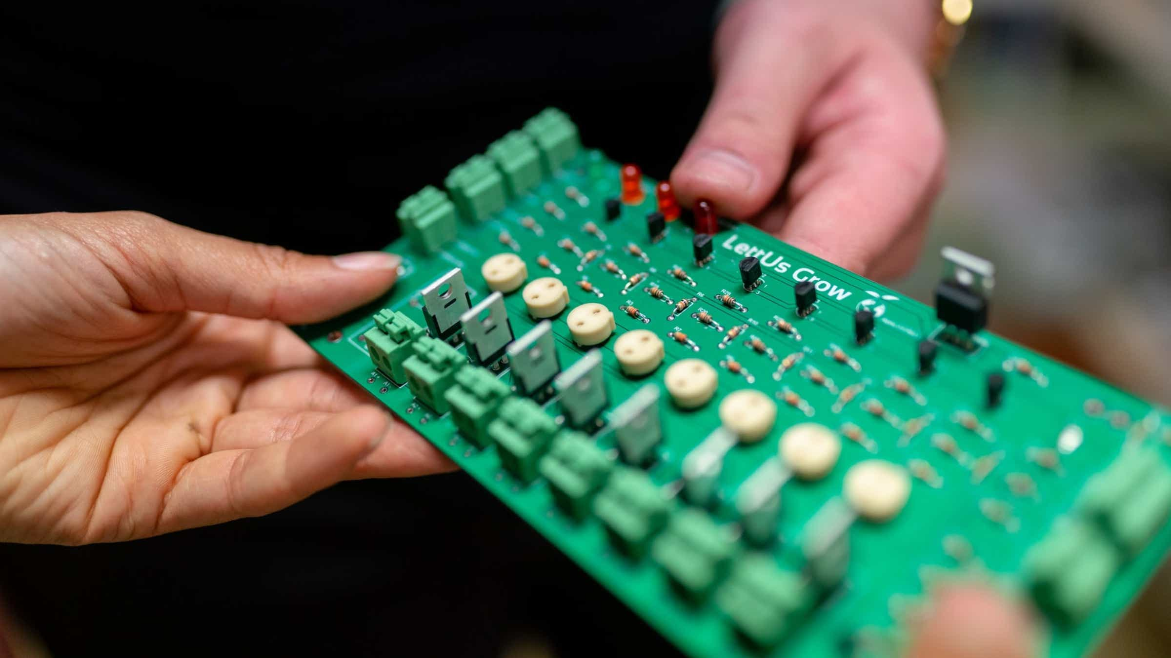
Develop physical design for the integrated circuit

(Task) Develop physical design for the integrated circuit
Description This OS unit is about developing the physical design for the integrated circuit by
converting the circuit design to geographical representation of different components.
It also includes design, verification and validation of the IC layout.
Scope This unit/ task covers the following:
Understand the work requirement
Understand the logic circuit design
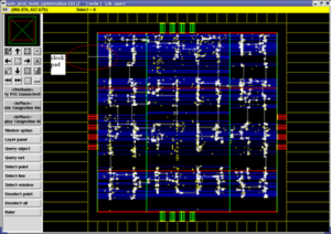
Develop physical design by following the design flow
Use software and tools for developing physical design
Coordinate with verification and testing engineer
Performance Criteria(PC) w.r.t. the Scope
Element Performance Criteria
Understanding work
requirement
To be competent, the user/ individual must be able to:
PC1. understand the work flow of the company’s design process
PC2. interact with the lead engineer in order to understand the work schedules,
shifts and delivery dates
PC3. plan work activities based the work flow and deliverables
PC4. understand broad level activities involved in the stages of design
PC5. list the various department to interact with for completing the work
PC6. minimise absenteeism and report to work on time
Understanding the
logic circuit design
To be competent, the user/ individual must be able to:
PC7. interact with project lead and design lead to understand the project specific
design mandate
PC8. understand the type of specific design requirement for integrated circuit
PC9. receive the circuit design from functional / logic design team
PC10. analyse and understand the circuit design
PC11. understand the design requirement i.e., fully custom design, semi-custom
design
PC12. identify library cells which may be used in the design

Developing physical
design
To be competent, the user/ individual must be able to:
PC13. define the physical design flow for the specific system
PC14. receive the verified and validated net list after the synthesis process
PC15. follow the defined physical design flow/steps sequentially to develop the IC
layout
PC16. perform floor planning which identifies the structures to be placed in the
layout
PC17. partition the chip into small blocks
PC18. ensure partition is done based on function/logic to enable easy placement
and routing
PC19. perform placement process after portioning